![[GlobalNews Home]](../globe.gif)
Up to now the only way to make one-dimensional quantum wires has been to grow two-dimensional quantum wells first, and then to use sophisticated process technology to define the wires. One of the drawbacks of the conventional approach has been that the processing can easily introduce impurities or unwanted damage into the structures.
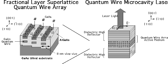
We used a different approach. When a GaAs crystal is cut slightly off one of its crystallographic orientations, a staircase-like pattern of regularly spaced nanometer-size steps naturally forms. We were able to grow layers of aluminum arsenide (AlAs) and gallium arsenide (GaAs) crystals, less than a monolayer in thickness, on top of the steps using chemical vapor deposition (CVD) growth technology. Using this technique, we succeeded in producing nanometer-order GaAs quantum wires. We call structures grown in this way fractional-layer superlattices.The deposition technique is unique in that it can create densely-packed quantum wires that can be precisely integrated into microcavity laser structures. The figure shows how the quantum wires are formed and how they fit into the microcavity laser structure.
Using an optical pumping technique to generate optical gain in the quantum wires, we were able to see strong monochromatic emission with a sharp threshold even at room temperature. This is the first time that lasing has ever been achieved in a quantum wire microcavity [Applied Physics Letters, vol.64, p.1759 (1994)]. The laser light exhibits polarization properties unique to the one-dimensional nature of the quantum wires. With further optimization of the laser structure, it will be possible to reduce the threshold current as well to demonstrate new switching capabilities which use polarization. We expect that quantum wire microcavity lasers will find wide application as light sources for optical data processing as well as optical communications.
Arturo Chavez-Pirson,
NTT Basic Research Laboratories
e-mail: chavez@wave.ntt.jp